
PCBA: From Bare Board to Ready-to-Use Electronic Assembly
A pcba turns an empty circuit board into a working electronic module, solving one of the most common challenges in product development and production: how to move from signal routing and component placement to a unit that can be installed directly into a device. For buyers, that difference matters. A bare PCB is only the foundation, while a populated board is the assembled platform that can shorten integration time, simplify procurement, and reduce in-house assembly workload.
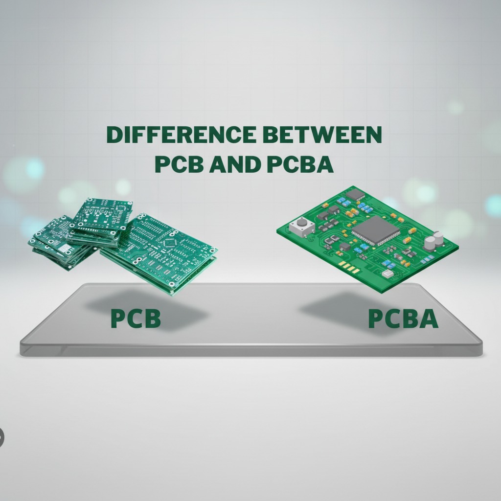
The image shows this contrast clearly. On the left is a bare printed circuit board with green solder mask, exposed pads, and plated holes. On the right is a completed board with an integrated circuit, surface-mount parts, connectors, and switch-style components. That visual comparison is useful for engineers, procurement teams, and OEM buyers who need to decide whether they require board fabrication only or a full PCBA制造 service.
Product Overview
A PCBA is the combination of a fabricated PCB and the electronic components mounted onto it. In practical terms, it is the assembled circuit stage between design and final product integration. The PCB provides the physical structure and copper pathways. The assembly process adds the active and passive parts that make the board function in a real device.
This distinction supports different buying needs. If a company has its own assembly line, it may purchase bare boards for internal mounting. If a project needs a quicker path to system integration, the assembled board is often more efficient. For prototypes, low-volume builds, and production programs alike, the right choice depends on how much of the electronics chain the buyer wants to outsource.
What Is Visible in the Board Structure
The bare PCB in the image has a rectangular shape, green solder mask, and visible copper features such as pads and vias. The board appears flat and laminated, which is typical of standard circuit board construction. While the exact laminate material is not confirmed, this type of board is commonly associated with fiberglass epoxy structures used across the electronics industry.
The assembled board shows a central IC, smaller SMD components, terminal-like parts, and at least one tactile button or switch. These elements indicate a mixed assembly approach that may include both surface-mount and through-hole features. Because the image is only an explainer, exact electrical performance, layer count, and component specifications should not be assumed.
Key Specifications and Capabilities
Bare PCB Capabilities
A fabricated PCB is designed to provide mechanical support and electrical interconnection. Its key roles include component mounting, signal routing, grounding, and power distribution. The board must also allow reliable solder attachment through plated holes, exposed pads, and surface finish areas prepared for assembly.
PCBA Capabilities
A completed pcba adds the functional building blocks of the circuit: chips, resistors, capacitors, connectors, switches, and any other specified parts. Once assembled, the board can be tested, integrated into a product enclosure, or used as a subassembly in a larger system. That makes it suitable for OEM products, industrial controls, consumer electronics, and development prototypes.
Decision-Driven Characteristics
Buyers usually evaluate a PCBA by compatibility, assembly completeness, component sourcing, board layout stability, and downstream integration requirements. For a bare PCB, the main concerns are fabrication quality, hole accuracy, copper integrity, and solder mask alignment. For the assembly stage, attention shifts to placement accuracy, soldering consistency, component orientation, and inspection coverage.
Materials and Finish Options
The image shows a green solder mask on both the bare board and the assembled board. Green remains one of the most common solder mask colors in electronics because it provides clear contrast for inspection and handling. Other finish and material options may be available depending on the project, but exact choices are not provided in the source data.
In a typical manufacturing context, PCB substrate options can vary by design needs, temperature demands, and electrical requirements. Surface finish selection may also affect solderability, shelf life, and assembly behavior. Since those details are not visible here, a buyer should confirm them during quotation and engineering review rather than assuming a standard configuration.
Manufacturing Process
PCB fabrication generally begins with a laminate panel that is drilled, patterned with copper, etched, and coated with solder mask. Plated holes and vias are created to connect traces between layers or through the board structure. The final bare board is then inspected and prepared for assembly.
PCBA制造 adds component placement and soldering. Depending on the design, this may include SMT placement for compact surface parts, through-hole insertion for connectors or switches, and reflow or wave soldering operations. After assembly, the board is typically checked for solder quality, placement accuracy, polarity, and visual defects. Additional electrical testing may be added according to project requirements, though no specific test package is stated in the supplied data.
Typical Application Scenarios
For engineering teams, a bare PCB is often used during prototype verification, design iteration, and in-house assembly programs. It gives the team flexibility to mount parts in their own facility or with a preferred contract manufacturer.
A finished pcba is better suited for buyers who want a board that can be installed directly into a final product or subsystem. Common use cases include control modules, embedded electronics, prototype devices, and OEM builds where speed and assembly consistency matter more than sourcing each stage separately.
That difference between bare board and assembled board is not just technical. It changes the purchase model, the inspection points, and the amount of labor still needed after delivery.
Quality Control Considerations
Quality control for PCB fabrication usually focuses on board geometry, surface cleanliness, solder mask coverage, copper continuity, drilling accuracy, and visual consistency. Any issue in these areas can affect downstream assembly and product reliability.
For PCBA, quality control expands to include solder joint appearance, component alignment, part presence, polarity verification, and basic functional checks if required by the build plan. Because the assembly contains active and passive parts, the risk profile is broader than that of a bare board. A buyer should therefore confirm what inspection steps are included before placing an order.
It is also important to align the bill of materials, approved component alternates, and assembly files before production begins. Even small differences in package style or footprint can create delays if not resolved early.
Customization Guidance for Buyers
When requesting a PCBA, the clearest starting point is the design package: Gerber files, BOM, pick-and-place data, assembly notes, and any special handling instructions. If the project requires a bare board only, the buyer should still specify stack-up expectations, board thickness, finish preference, and panel requirements when available.
Buyers should also decide how much of the sourcing chain they want managed by the supplier. Some projects need only assembly. Others require component procurement, test support, or revision control. The right scope depends on internal engineering capacity and production schedule.
If the design is still changing, it is often wise to discuss prototype quantities before scaling into production. That helps reduce rework and lets the engineering team confirm fit, solderability, and board-level behavior before committing to larger volumes.
How to Choose Between PCB and PCBA
The choice comes down to workflow. A bare PCB suits teams that want to control assembly themselves or need boards as a starting point for development. A completed pcba suits teams that want a functional electronic assembly ready for the next step.
Several factors usually guide the decision: available assembly capacity, project schedule, component supply complexity, testing needs, and the level of integration required in the final product. If the goal is to accelerate delivery and reduce internal labor, the assembled board is usually the more practical option. If the goal is engineering flexibility or independent sourcing, the bare board may be the better fit.
Why the Difference Matters in Real Production
In real manufacturing, the gap between a bare PCB and a populated assembly can determine how many process steps remain before shipment. A board without components is easier to store and ship, but it is not yet a usable electronics unit. Once components are mounted and soldered, the board becomes a more complete production asset, ready for integration into the system architecture.
That is why buyers comparing PCB and PCBA should think beyond the board itself. They are really choosing between a fabrication input and a functional assembly output.
Contact for PCB and PCBA Requirements
If you need a bare PCB for internal assembly or a finished pcba for direct integration, start with your design files and build requirements. Share the intended board type, component list, and production scope so the manufacturing route can be matched to the project. Clear inputs lead to clearer quotations, smoother assembly planning, and fewer surprises during production.
For OEM programs, prototypes, and contract manufacturing projects, the best next step is to request a review of the board structure, assembly scope, and documentation set before production begins.





评价
Clear filters目前还没有评价