
PCBA for Electronics That Need to Move from Bare Board to Working Assembly
When a design reaches the point where a bare board is no longer enough, pcba becomes the practical answer. It solves a common buyer problem: turning a printed circuit board into a populated electronic assembly that can be tested, integrated, and installed into a device with far less internal handling. For OEMs, procurement teams, and electronics engineers, the difference between a PCB and a PCBA is the difference between a structural platform and a functional module.
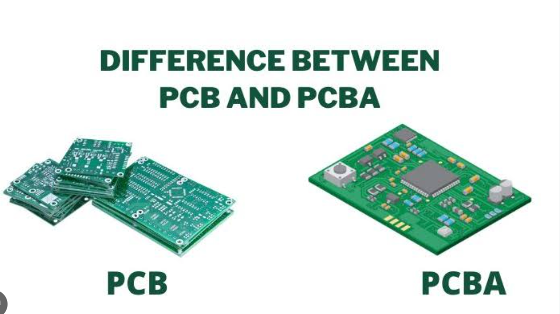
The image shows that distinction clearly. One board is an unpopulated PCB with exposed traces, pads, and mounting holes. The other is a PCBA with mounted components, including a central IC, smaller passive parts, and a switch-like device. Both are rigid green boards, but only the assembled one is ready for the next stage of product integration. That is why PCBA manufacturing is often selected when the project needs a board that can do more than simply carry copper routes.
Product Overview
A PCBA, or assembled printed circuit board, starts from a fabricated PCB and then receives electronic components through assembly operations. In practical terms, the bare PCB provides the mechanical support and electrical pathways, while the assembly step gives the board its working function. This makes PCBA a central supply item for control electronics, embedded devices, and product prototypes that must be evaluated in a real operating environment.
For buyers comparing bare-board supply with assembled-board supply, the decision usually comes down to project stage and internal capability. If your team only needs the substrate, PCB fabrication is enough. If you need a board that can be installed into a device, validated in a circuit, or used as part of a finished module, PCBA is the more complete delivery format.
What the Visible Structure Tells Buyers
Bare PCB
The unpopulated board in the image shows several useful features that buyers can inspect visually: drilled mounting holes, copper trace patterns, and exposed pads for future component attachment. This kind of board is the starting point for custom electronics, prototype runs, and production control boards. Its green solder mask finish is a familiar choice in electronics manufacturing and helps define the protected copper areas while leaving pads available for electrical connection.
PCBA
The assembled board adds the layer that changes everything: components are mounted and soldered onto the board. In the visible example, the PCBA includes a central integrated circuit or package, smaller passive components, and at least one button or switch-like part, along with contact pads and other connection points. Even without knowing the final end product, the board already communicates a clear message: this assembly is prepared for functional use rather than further basic fabrication.
Key Specifications and Capabilities
Because the supplied image does not show all engineering data, it is best to discuss PCBA in terms of verifiable and configurable attributes rather than fixed claims. Typical buyer-facing considerations include board size, layer count, copper distribution, component density, interconnect style, and the mix of assembly steps required. In this case, the visible product is a rigid rectangular board with a green finish, and the populated version demonstrates a compact component arrangement suitable for electronic integration.
PCBA manufacturing can support a wide range of board functions depending on the design. Some assemblies are simple and use only a few components; others are dense with ICs, connectors, sensors, and support circuitry. The actual performance depends on the schematic, bill of materials, fabrication data, and assembly controls rather than the board format alone.
Materials and Finish Options
The boards shown use a green solder mask, which is the most recognizable finish in many electronics environments. Solder mask is not just visual; it helps protect copper features and guides solder placement during assembly. The final appearance may vary by project, but the key idea remains the same: finish choice affects manufacturability, inspection clarity, and the way the board handles assembly steps.
Material selection for the PCB base is not identifiable from the image, so it should be defined during engineering review. Buyers commonly specify the substrate and surface finish according to operating needs, component pitch, and expected assembly method. For PCBA projects, it is important that material and finish choices align with solderability, reliability, and downstream device constraints.
Manufacturing Process: From PCB Fabrication to PCBA
PCBA is built in stages. First comes PCB fabrication, where the board is formed, holes are drilled, and copper patterns are created. The bare PCB in the image reflects that stage clearly. After fabrication, the assembly process begins. Components are placed on the board, then fixed through soldering operations that may include SMT, through-hole assembly, or a combination, depending on the design. The image confirms that the populated board includes soldered terminations, but it does not reveal the exact process mix, so that should be finalized by the manufacturing plan.
After assembly, the board generally moves through inspection and testing steps appropriate to the product. These may include visual inspection, electrical checks, and function verification based on the buyer’s requirements. For procurement teams, the value of a single PCBA source is that it consolidates multiple workstreams into one managed output.
Application Scenarios
PCBA is used wherever a circuit needs to become a usable electronic unit. That includes control boards, embedded modules, interface boards, prototype validation assemblies, and production electronics for industrial or consumer devices. The bare PCB, by contrast, is the foundation for custom electronics development and early-stage trials.
This makes the product relevant to several buyer groups. OEMs may need repeatable assembly for device production. Electronics designers often need a prototype PCBA to verify a schematic in real hardware. EMS providers may source the board as part of a larger build program. Procurement teams frequently compare PCB-only supply with PCBA supply to manage cost, lead time, and in-house assembly capacity.
Quality Control Considerations
Quality control in PCBA manufacturing starts with accurate fabrication and continues through component placement and soldering. The assembled board must maintain clean pad wetting, solid attachment, and consistent alignment. The bare board must also support the assembly process without defects that could affect mounting or connectivity. Since the provided data does not include measured quality metrics, it is better to evaluate suppliers through process controls, inspection methods, and sample review rather than assumptions.
When evaluating a PCBA source, buyers should ask how incoming materials are checked, how solder joints are inspected, and what level of electrical or functional testing is offered. These questions matter more than appearance alone, especially for boards that will operate inside a finished product.
Customization Guidance for Buyers
PCBA projects are usually customized around the end application. Before placing an order, define the electrical requirements, the target enclosure, connector locations, and the expected assembly complexity. A board with a few components has very different manufacturing needs than a densely populated control module. If the project begins as a PCB-only design, confirm whether assembly support will be added later or sourced together from the start.
It also helps to share the complete technical package early: Gerber files, BOM, assembly drawings, and any notes on component orientation or special handling. Clear documentation reduces ambiguity and helps the manufacturer match the PCB fabrication stage with the assembly stage more smoothly. For PCBA, that coordination is often where lead-time risk and quality risk are reduced.
How to Decide Between PCB and PCBA Supply
If your team has in-house assembly capability, a bare PCB may be the right choice. If your objective is a board that can be installed directly into a device or used for system evaluation, PCBA is usually the more efficient path. The choice is not only about price; it is also about labor, test readiness, and how much work remains before the board can serve its intended purpose.
Another practical factor is consistency. A populated assembly built to the same documentation can help standardize prototypes and production units more effectively than manually assembled boards. For buyers managing multiple revisions, the PCBA format often makes it easier to track changes in components and layout from one build to the next.
Request PCBA Support for Your Next Build
If you are comparing PCB fabrication with PCBA manufacturing, start by defining where your project sits today and what the board must do next. A bare PCB gives you the foundation; a PCBA gives you a working electronics assembly. Share your design files, outline your component requirements, and confirm the needed assembly scope so the build can move from layout to usable hardware with fewer surprises.
For OEM sourcing, prototype development, or production planning, PCBA is the format that bridges design intent and real-world function. Send your board requirements and ask for a manufacturing review to match the right fabrication and assembly approach to your project.







评价
Clear filters目前还没有评价